Author: Denis Avetisyan
A new approach uses graph neural networks to automatically balance and optimize the complex patterns needed for modern microchip design.
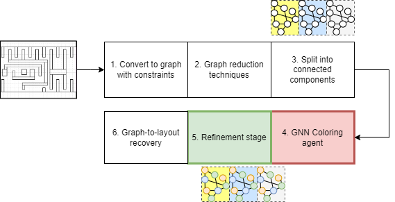
This paper details an unsupervised graph neural network framework for improved multipatterning and constraint satisfaction in advanced electronic design automation.
Achieving dense circuit layouts in modern electronic design automation often clashes with lithographic limitations, necessitating complex decomposition strategies. This paper introduces ‘Unsupervised Graph Neural Network Framework for Balanced Multipatterning in Advanced Electronic Design Automation Layouts’, a novel approach framing multipatterning as a constrained graph coloring problem. By integrating unsupervised graph neural networks with iterative refinement, the framework achieves both conflict-free layout decomposition and balanced mask usage. Could this data-efficient pipeline represent a scalable baseline for future EDA workflows and unlock even denser integrated circuit designs?
The Inevitable Limits of Shrinking Things
The relentless drive for more powerful and compact electronics faces a fundamental hurdle: the limits of lithography. As transistors shrink and circuit density escalates, traditional single-pattern lithography-the process of transferring circuit designs onto silicon wafers-struggles to achieve the necessary resolution. This isn’t merely a technical inconvenience; the inability to precisely define these minuscule structures directly impacts both performance and cost. Imperfectly formed transistors operate less efficiently, slowing down processing speeds and increasing energy consumption. Furthermore, attempting to circumvent these limitations with increasingly complex and expensive lithography tools – or accepting lower yields due to manufacturing defects – significantly raises the final cost of integrated circuits, potentially hindering innovation and accessibility in the broader technology landscape.
As the demand for increasingly powerful and compact microchips intensifies, the manufacturing process faces significant hurdles, particularly concerning the resolution limits of traditional lithography. To circumvent these constraints, a suite of innovative layout decomposition techniques, broadly termed multipatterning, has emerged as a crucial necessity. This approach doesn’t attempt to force a single, intricate design onto the silicon; instead, it strategically dissects the complex layout into a series of simpler, more manageable patterns. Each of these simplified patterns is then applied sequentially, utilizing multiple photomasks and fabrication steps. Through this iterative process, features are gradually built up, effectively bypassing the resolution limitations of single-pattern lithography and enabling the continued miniaturization of electronic devices. The success of multipatterning, however, relies heavily on sophisticated algorithms and precise control over each fabrication step to ensure accurate pattern alignment and minimize defects.
Multipatterning addresses the escalating challenges of modern chip fabrication by strategically dissecting intricate circuit designs into a series of more manageable layers. This process isn’t about improving a single step, but rather fundamentally restructuring how chips are built; instead of attempting to etch all features in one go, the layout is decomposed. Each simplified pattern is then transferred onto the silicon wafer using a separate photomask and etching process. This sequential application of multiple masks allows manufacturers to bypass the resolution limitations of single-pattern lithography, effectively doubling or even quadrupling the density of transistors on a chip. While increasing complexity and cost, multipatterning remains a vital technique for continuing the advancement of computing power and shrinking device dimensions, enabling the creation of increasingly sophisticated integrated circuits.
Decomposing the Problem: A Graph Coloring Analogy
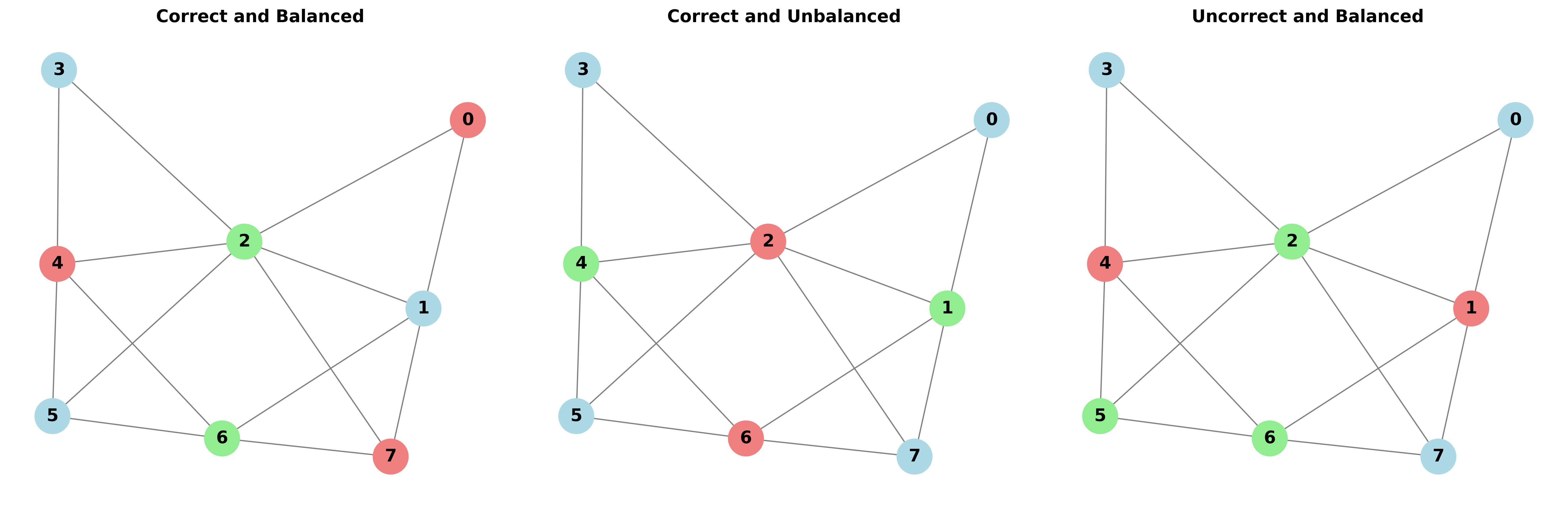
The decomposition of integrated circuit layouts for multipatterning lithography can be formally represented as a constrained graph coloring problem. In this model, individual circuit features – such as polygons representing transistors or interconnects – are defined as the nodes of a graph. Each required lithographic mask is then represented as a color. The assignment of a mask (color) to a feature (node) signifies that the feature will be defined by that specific mask. This allows for a mathematical framework to address the layout decomposition problem, enabling the use of graph coloring algorithms to determine an optimal mask assignment.
The decomposition process, when framed as a constrained graph coloring problem, necessitates assigning each circuit feature – representing a node in the graph – to a specific mask, which corresponds to a color. This assignment is not arbitrary; design rules impose constraints that define which features are incompatible and, therefore, cannot be assigned to the same mask. These constraints are represented as edges between nodes, indicating that connected features must be assigned different colors. The validity of a solution hinges on satisfying all such constraints, ensuring no design rule violations occur during multipatterning lithography. Successfully coloring the graph, while adhering to these rules, determines a feasible decomposition with a minimized mask count.
Employing established graph coloring algorithms for layout decomposition leverages the well-studied properties of chromatic numbers and heuristics. Algorithms such as greedy coloring, DSatur, and more sophisticated approaches like simulated annealing or genetic algorithms can be adapted to assign features (graph nodes) to masks (colors) while satisfying design rule constraints (graph edges defining conflicts). The minimization of mask count directly correlates to minimizing the chromatic number of the graph; therefore, algorithms focused on finding lower bounds for chromatic numbers, or efficiently exploring the solution space, become critical for optimizing multipatterning layouts. Performance is further impacted by the graph’s density and connectivity, necessitating algorithm selection and parameter tuning tailored to specific layout characteristics.
The Delicate Art of Mask Balancing
Color balancing, the equitable distribution of design features across reticle masks, directly impacts manufacturing efficiency and cost. Uneven feature distributions necessitate more complex mask handling procedures, increased inspection requirements, and potentially, the use of more expensive mask materials to accommodate variations in feature density. Specifically, significant imbalances can lead to differing levels of optical proximity correction (OPC) across masks, complicating lithographic processes. By minimizing the disparity in feature counts and sizes between masks, color balancing reduces these complexities, streamlines manufacturing workflows, and ultimately lowers production costs. The goal is to ensure each mask receives a representative and manageable workload during the lithographic process.
Simulated annealing is a probabilistic metaheuristic optimization algorithm used in mask assignment to iteratively improve solution quality. The process begins with a random initial assignment of shapes to masks, and subsequently explores the solution space by making small, random changes to this assignment. These changes are accepted based on a probability determined by both the change in a cost function – which quantifies design rule violations and color imbalance – and a “temperature” parameter. Higher temperatures allow for acceptance of worse solutions, facilitating escape from local optima. As the temperature gradually decreases, the algorithm converges towards a low-cost, balanced mask assignment. This iterative refinement continues until a stopping criterion is met, typically a sufficiently low temperature or a negligible improvement in the cost function.
The implemented Graph Neural Network (GNN)-based approach consistently achieves a 100% solve rate across both training and test datasets, indicating robust generalization capability. This represents a significant performance improvement compared to classical algorithms used for mask assignment optimization. Quantitative validation is provided by the achieved average balancing error of 1.716, a metric used to assess the distribution of features across masks; lower values indicate better balance and reduced manufacturing complexity. This low error rate confirms the effectiveness of the GNN in minimizing design rule violations and optimizing mask assignments.
Standardizing the Benchmarks: The OpenMPL Framework
The development of the OpenMPL framework addresses a critical need for standardized benchmarking in multipatterning lithography. Prior to its creation, comparing the efficacy of different algorithms proved challenging due to inconsistencies in graph generation and a lack of reproducible instances. OpenMPL provides a systematic approach to creating these benchmark datasets, ensuring that any algorithm evaluated operates on the same foundational graph structure. This standardization is achieved through a defined process for generating graph instances from real-world design data, allowing researchers and developers to fairly assess and compare the performance of their multipatterning algorithms. By eliminating variability in the input data, OpenMPL facilitates objective evaluation, accelerating progress in the field and enabling the identification of truly superior approaches to resolving complex layout patterns.
The ILP_UPDATED algorithm, a core component of the OpenMPL framework, tackles the complex challenge of multipatterning optimization by framing it as a graph coloring problem solvable through integer linear programming (ILP). This approach represents each lithographic pattern as a node in a graph, with edges connecting conflicting patterns – those that, if applied simultaneously, would violate design rules. The ILP formulation then seeks to assign each node (pattern) a color (mask assignment) such that no adjacent nodes share the same color, effectively minimizing conflicts. By leveraging established ILP solvers, ILP_UPDATED systematically generates optimized mask assignments, providing a benchmark against which novel algorithms – such as graph neural networks – can be rigorously compared. The resulting solutions demonstrate the feasibility and effectiveness of using mathematical optimization to address critical challenges in advanced lithography.
The developed graph neural network (GNN)-based algorithm achieves a high success rate in resolving complex multipatterning challenges, demonstrating the ability to generate valid mask assignments for 83.64% to 100% of benchmark instances, contingent on specific configuration parameters. Critically, the algorithm maintains exceptional balance in the resulting mask assignments, quantified by a balancing error consistently falling between 1.81 and 2.31. These performance metrics represent a significant advancement over traditional, classical methods employed in multipatterning optimization, highlighting the GNN’s capacity to efficiently navigate the intricate solution space and deliver superior results with minimized imbalance-a crucial factor for lithographic process control and pattern fidelity.
Pushing the Limits: Beyond Quadruple Patterning
The relentless pursuit of more powerful and compact integrated circuits necessitates a continuous reduction in feature size. As dimensions shrink towards the single-digit nanometer scale, traditional lithographic techniques reach their physical limits. This has driven increasing interest in higher-order multipatterning, most notably quadruple patterning (QP), and even techniques beyond. These methods involve using multiple photolithographic masks to define intricate patterns on silicon wafers, effectively doubling or even quadrupling the achievable resolution. The demand for QP and its successors isn’t merely a technological aspiration; it’s a fundamental requirement for sustaining Moore’s Law and enabling continued advancements in computing, communication, and countless other technological domains. Without these sophisticated patterning approaches, further miniaturization-and the performance gains it delivers-becomes increasingly unattainable.
Quadruple patterning (QP) represents a significant leap in microfabrication, enabling the creation of incredibly dense and high-resolution integrated circuits. This technique achieves such precision by employing four separate photomasks to define a single layer of the circuit, effectively quadrupling the potential resolution. However, this increase in complexity isn’t without its hurdles. The algorithmic challenges associated with QP are substantial; determining the optimal sequence and configuration of these masks requires navigating a vast solution space. Optimization becomes critical to minimize errors and ensure manufacturability, demanding sophisticated computational frameworks capable of balancing competing priorities like resolution, density, and yield. Successfully addressing these challenges is paramount to continuing the trend of miniaturization in the semiconductor industry and unlocking the potential of next-generation microchips.
Recent advancements in computational lithography demonstrate a robust pathway toward continued integrated circuit miniaturization. Utilizing novel techniques and frameworks, researchers have achieved a 100% resolution enhancement solve rate – meaning every design challenge presented was successfully addressed – while simultaneously minimizing average balancing error to just 1.716. This level of precision is critical for quadruple patterning and beyond, as it directly impacts the manufacturability and reliability of increasingly dense chip designs. The demonstrated efficacy provides a solid foundation for tackling the algorithmic complexities inherent in high-order multipatterning, ultimately enabling the creation of smaller, faster, and more energy-efficient electronic devices.
The pursuit of automated layout optimization, as detailed in this work concerning graph neural networks and multipatterning, feels destined to join the ranks of elegantly complex systems ultimately defeated by the realities of production. It’s a familiar story. The framework attempts to balance coloring and constraint satisfaction, a noble goal, but one invariably challenged by unforeseen interactions and the sheer scale of modern designs. As Linus Torvalds once said, ‘Most developers think lots of coding time means lots of functionality. That’s a lie.’ This research, while innovative in its approach to unsupervised learning, will undoubtedly reveal its own set of limitations when faced with the relentless demands of real-world EDA. One can almost predict the emergence of ‘graph neural network debt’ – a new layer of complexity to manage. The system might crash consistently, at least it’s predictable, and leaves notes for digital archaeologists.
What’s Next?
The elegance of framing multipatterning as a graph coloring problem, and then automating constraint satisfaction with a neural network, is… predictable. It will work, until production finds a way to make it exquisitely, painfully not work. The current framework addresses balancing and coloring, which is good. But anyone who’s stared down a reticle knows the real problems aren’t the algorithms; they’re the corner cases, the stochastic effects, the sheer volume of data. Expect future iterations to focus less on clever networks and more on robust data handling, and a graceful degradation when the inevitable happens.
The unsupervised approach is a smart move, sidestepping the need for painstakingly curated training data. Yet, the line between ‘unsupervised’ and ‘unconstrained’ is often blurred. It’s likely that the true gains will come from hybrid models – leveraging unsupervised pre-training, then fine-tuning with limited, targeted supervision. Because, ultimately, someone will always need to explain to the system why that particular shape is impossible.
This work will become legacy, of course. A memory of better times, when the problem seemed tractable. The next challenge isn’t just automating the layout, but automating the adaptation to the inevitable failures. Perhaps a system that doesn’t ‘solve’ the layout, but rather prolongs its suffering, slowly nudging it toward something… acceptable. That feels more realistic.
Original article: https://arxiv.org/pdf/2511.16374.pdf
Contact the author: https://www.linkedin.com/in/avetisyan/
See also:
- Building 3D Worlds from Words: Is Reinforcement Learning the Key?
- Spotting the Loops in Autonomous Systems
- The Best Directors of 2025
- The Glitch in the Machine: Spotting AI-Generated Images Beyond the Obvious
- 2025 Crypto Wallets: Secure, Smart, and Surprisingly Simple!
- Umamusume: Gold Ship build guide
- 20 Best TV Shows Featuring All-White Casts You Should See
- Mel Gibson, 69, and Rosalind Ross, 35, Call It Quits After Nearly a Decade: “It’s Sad To End This Chapter in our Lives”
- Gold Rate Forecast
- Uncovering Hidden Signals in Finance with AI
2025-11-24 02:40